Resistivity Theory:
1. Purpose:
To determine the Resistivity of a substrate or a thin film by using the four point probe, current source. This SOP also determines the conductivity using the four-point probe.
2. General Instructions and Precautions:
The probe tips are a very critical part of the four-point probe and great care should be taken when using the equipment. Two different materials are used for the probe tips. Tungsten Carbide is a crystalline material, which is very hard and somewhat brittle. If the wafer is moved horizontally while the probe arm is down, the Tungsten Carbide tips tend to break off in little pieces. The second material, osmium, is also a hard material but does not chip. When mishandled, the entire tip can be broken. Osmium tips cost more than Tungsten Carbide and is the kind used in the four-point probe system.
3. Resistivity Theory
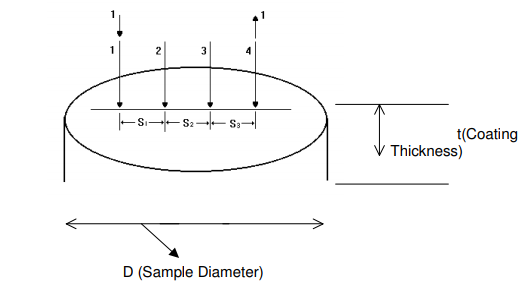
The four-point probe is preferable over a two-point probe because the contact and spreading resistance associated with the two-point probe can’t be measured. This means that the true sheet resistance can’t be accurately separated from the measured resistance. The four point probe consists of two current carrying probes (1 and 4), and two voltage measuring probes (2 and 3) (refer to schematic). Since very little contact and spreading resistance is
associated with the voltage probes, one can obtain a fairly accurate calculation of the sheet resistance, which is then used to calculate the Resistivity. The Resistivity (p) of a semi-infinite wafer with equal probe spacing (s) is given by:
p=2*pi*s*V/I
Since wafers are not semi-infinite in extent, the right hand side of this equation must multiply a combination of correction factors. By following the procedure below, the need for many of these factors is eliminated. The correction factors still needed, and the final forms of the formulas for sheet resistance and Resistivity are given below in the procedure section.
4. Resistance correction factor :
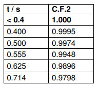
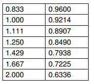
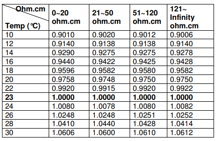
Sheet Resistance (RS) = p/t= (V/I) X C.F.1 X C.F.2 X C.F.3
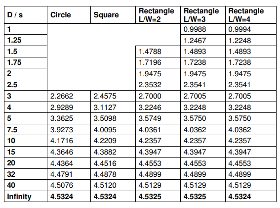
Where p is the Resistivity is the thickness of the sample, and C.F.1 is the sheet resistance correction factor, which depends on the wafer diameter (d) and the probe tip spacing (s). For the UofL setup, s is equal to 62.5 mils. If the
ratio of d/s is greater than 40, the sheet resistance correction factor levels off at 4.5324. If the ratio is less than 40, use the table below [3] to determine the appropriate correction factor. In the rectangle columns, the number refers to the length to width ratio, with the length being the longer of the two sides. The rectangle 4 column refers to a ratio greater than or equal to 4. Rectangular samples should be tested with the length parallel to the probe tips and the
width should be taken as d when determining the correction factor. s is the spacing between the probe tips (62.5 mils for UofL setup and C.F.2 is the Resistivity correction factor. C.F.2 is given in the table below. For the case when t is much less than s (less than 4/10 of s), C.F.2 is simply equal to unity.
[1] Note: the above equation and the table are only valid for junctions diffused on one side of the sample. A chemical source will diffuse both sides, which means the back side must be removed to use these factors, or different factors must be used.
C.F.3 is Temperature Correction Factor.
Sample Size Correction Factor (C.F.1)
Sample Thickness Correction Factor (C.F.2)
Temperature Correction Factor Table (C.F.3)
Références.
1. L.B. Valdes. Proc. 3T,R.E. 42 (1954) p. 420-427
2. J.K. Hargreaves and D. Millard. Brit. J. Appl. Phys. 13 (1962) p. 231-234.
3. C.L. Paulnack and N.J. Chaplin. Rev. Soi. Instr. 33 (1962) p. 873-875.
4. E.B. Hansen. Appl. Soi. Res. Sect. B, 8 (I960)p. 93-104-
5. P.M. Smits. Bell System Tech. J. 37. (1958) p. 711-718.
6. A. Unliry, Jr. Bell System Tech. J. 34 (1955) p. 105-128,
7. A. Uhlicr.,, Jr. Bell System Tech. J. 34 (1955) p. 994.
8. l.J. Swartzendruber. National Bureau of Standards, Tech.; Note 199, April 15, 1964.
9. M.A. Logan. Bell System Tech. J. 40 (1961) p. 885-919.
10. J. Swartzendruber. Solid State Electronics. 7,(1964) p. 413-422.