CV / IV Analysis system
C-V / I-V Analysis Systems for Semiconductor R&D and Process Development
MDC Europe offers high-performance systems for advanced semiconductor device characterization. Our solutions cover essential measurements including CV (capacitance-voltage), IV (current-voltage), conductance, and gate oxide integrity. We specialize in providing precise doping and resistivity profiles, as well as mobile ion concentration (TVS) analysis. Our systems are fully customizable, integrating top-tier meters (Agilent, Keithley, HP) with specialized probing stations to monitor critical processing steps, detect contamination, and ensure material quality in both research and industrial environments.
Our Probes Solutions
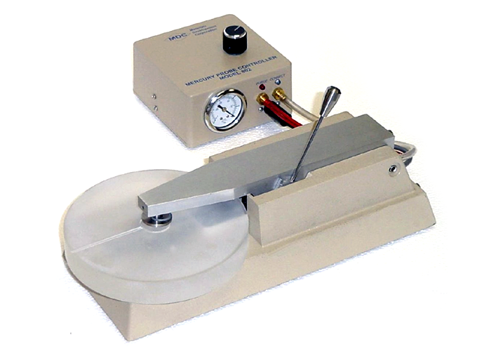
Engineered for non-destructive C-V, I-V, and sheet resistance characterization. These systems are essential in R&D and process development where permanent metallization is not desirable or possible. They allow for rapid characterization, materials research, and early-stage device evaluation, providing a fast track to identifying furnace contaminants and epitaxial layer quality without damaging the wafer.
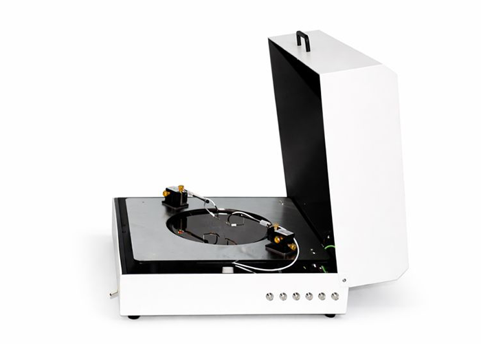
Precision temperature-controlled probing solutions designed to enable stable electrical measurements under defined thermal conditions (up to 400°C). The QuietChuck technology is specifically engineered to eliminate electrical noise and AC interference, making it ideal for sensitive temperature-dependent C-V / I-V analysis. These systems are the industry standard for mobile-ion monitoring (BTS tests) and gate oxide reliability workflows in demanding test environments.
Your Needs, Our Solutions
Junction Characterization
- C-V Plotting
- Doping Profiling
- Resistivity Profiling
- Average Doping or Resistivity Function
- Find Flat Zone Function
- Q-V Plotting
- Doping-Voltage Plotting
- Series Resistance Correction
- 1/C²-V Plotting
- 2DEG Analysis
MOS Characterization
- C-V Plotting
- Swept, Pulsed, Retrace & Hysteresis
- Dual Frequency Mode for Leaky Oxides
- Inversion Layer Stabilization
- Series Resistance Correction
- Conductance-Voltage Plotting
- Theoretical MOS C-V Plots
- CVC Computations for Thin Oxides
- Quantum Modeling using CVC
- Polysilicon Depletion Modeling using CVC
- Dielectric Constant Mode
- Ricco Analysis for Thin Oxide Parameters
- Sub-Oxide Doping Profiling (Ziegler)
- Implant Profiling
- Partial Dose Integration
- Mobile Ionic Charge (CVBT Method)
- Tests for Valid/Invalid CVBT Shifts
- Overlay Plots
- Production Version
Capacitance-Time Characterization
- C-T Plots
- Lifetime-Depth Plots
- Zerbst Plots
- Automatic Time Selection Mode
Conductance-Voltage-Frequency Plots
- C-F Plots
- G-F Plots
- Dit-V Plots
- Nicollian-Goetzberger Analysis
- G(F,V) Plot Families
- C(V,F) Plot Families
Quasi Statics C-V Plots
- Leakage Correction
- Offset Correction
- Theoretical Plots
- Alternate CVC Computations
- Quantum Modeling using CVC
- Polysilicon Depletion Modeling using CVC
Capacitance - Surface Potential Plots
- Find Bergland Integration Constant
- Dit versus Surface Potential using Kuhn Method
- Dit versus Energy using Kuhn Method
- Dit versus Surface Potential using Castagne Method
TVS Plots
- Mobile Ionic Charge Concentration
- Mobile Ionic Charge Species
- Plot C-V or I-V
- Find Peak Current
- Production Version
Current versus Voltage Plots
- Plot Current versus Voltage
- Fowler Nordheim Analysis for Thin Oxides
- Junction Characteristics for pn or Schottky Barriers
- Pulsed I-V Measurement Mode
- Current-Time Plots for Cu Diffusion Studies
- PV Mode for Solar Cells – Finds Pmax, Rs, Rsh, FF
GOI Tests
- Force Constant Voltage (TDDB-V)
- Force Ramped Voltage (TZBD)
- Force Constant Current (TDDB-I)
- Force Stepped Voltage (JT)
- Pulsed Voltage Source (PVBD)
- Pulsed Voltage Wearout (TDDW-V)
- Pulsed Current Wearout (TDDW-I)
- Fixed Voltage
- Analyses :
- Histograms
- TDDB Plots
- JT Plots
- Qbd Plots
- Weibull Plots
- 3D Surface Plots with Probers
- Wafer Maps with Probers
Dielectric Constant Tests
- Find Permittivity
- Find Loss Factor
Probe Station Interfacing
- Standard Hot Chuck
- Prober with Stepping
- Prober with Autoloading
- Glove Box for Oxygen-Free Measurements
- QuietCHUCK with Hermetic Enclosure for Oxygen-Free Measurements
- Mercury Probes for Rapid Non-Destructive Measurements
- Cryogenic Prober for Low Temperature Measurements
Special Functions
- Production Resistivity Measurements
- Production TVS Measurements
- Implant Modeling
- SPC
- Generation Lifetime
- Multiple Measurement Sequencing
- Electromigration
- Parametric Testing
TFT or Transistor Test Suite
- Transfer Characteristics
- Saturation Characteristics
- Output Characteristics
- Leakage Tests
- Conductivity Tests
Calculations
- Parallel Plate Capacitor
- Doping-Resistivity
- Depletion-Doping-Voltage
- Breakdown Voltage-Doping
Four Point Probe Tests
- Resistance
- Resistivity
- Sheet Resistance
- Doping
Multiple Material Parameters
- Permittivity
- Bandgap
- Electron Affinity
- Mobility
Drive Level Capacitance Profiling
- C-V Plot Family
- Defect Density Profiles
- Standard CV Profiles
- Variable Frequency
- Variable Temperature
Why MDC Europe?
MDC Europe combines decades of expertise in semiconductor metrology with highly flexible system configurations. We provide end-to-end application support, ensuring that our C-V / I-V analysis solutions are perfectly tailored to meet the rigorous requirements of advanced research centers and semiconductor fabrication plants worldwide.
Why to Choose Our Products?
- OEM-level refurbishment meeting original specifications
- 30+ years of experience in semiconductor solutions
- Fast European delivery and support
- Comprehensive product portfolio from spares to systems
- Trusted by leading OEMs and research institutes